Research and Development Projects
|
We are working in the following research areas with different local and international partners. Integrated Bio-GMI Sensor and Electronics (In-progress) Funding Agency:
This project proposes a high-sensitivity, miniaturized and low-cost bio-sensor system for blood-assay and pathogen detection for point-of-care testing (POCT). The proposed system would enable early-stage detection of infectious diseases by driving technological developments towards low cost, easy to use and accurate portable electronic systems for medical diagnosis. The complete bio-sensor system would consist of a GMI (Giant Magneto Impedance) sensor, an application-specific readout IC (ASIC) developed to provide electrical and mechanical interface to the GMI sensor. The system would target specific diagnostic bio-markers and biological linkers to modulate the sensor’s impedance through magnetic coupling for selective detection. The GMI sensor would be integrated with the readout ASIC in an appropriate package to reach an area-efficient footprint. The ASIC would be custom-designed and fabricated in CMOS process through a standard CMOS FAB.
Point-of-Care Electronic Test Kit for Rapid Detection of Pathogens using Graphene-Transistors as Biosensors (In-progress) Funding Agency:
This project proposes the development of ahand-held point-of-care electronic test-kit for rapid pathogen detection (termed as the front-end), which is supported by a backend server employing Artificial Intelligence. This front-end would be similar to a hand-held Glucometer with disposable sensor-strips and a battery-operated reusable reader/teller with internet connectivity. The backend server would bea high computation-power platform with cloud connectivity and data-storage placed at a centralized site.
Indigenous design and manufacturing of full flight motion platform (In- Progress) Funding Agency:
The motion-actuated platform is an indigenously designed first-of-its-kind motorized full flight simulator. Covering high ranges of rotation and a distinct feature of mimicking the performance and rates of multiple large aircrafts. The motorized feature gives us a greater edge to control the inertia, momentum, torque, acceleration and speed of the platform which enables us to cover a wide range of aircrafts. The simulator comes equipped with our multi-axes motion platform which demonstrates a robust and accurate depiction of an aircraft’s deflection and turbulent behavior in the pitch, roll, yaw and heave axes.
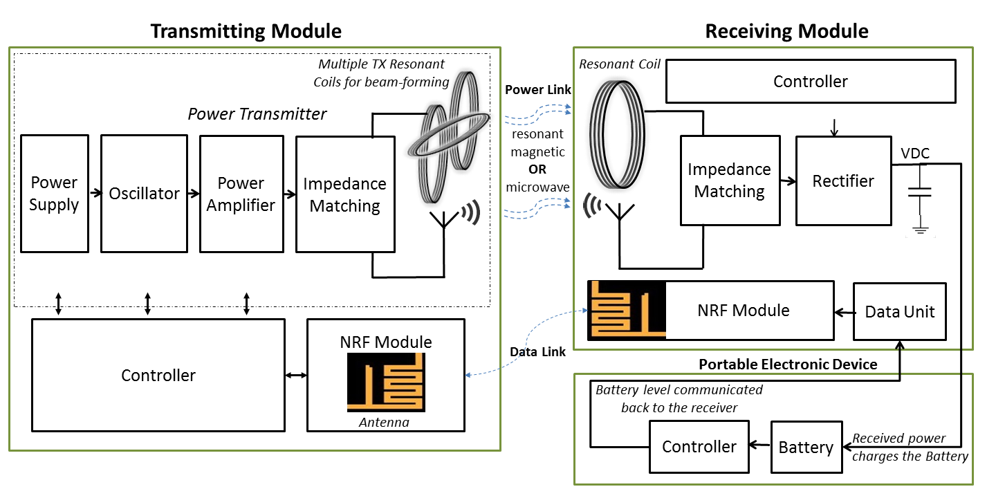
A Mid-Range Wireless Power Transfer System For PortableElectronic Devices With Beam Forming (Completed) Funding Agency;
This project encompasses the relevant data and information that was referred to and was used to design, fabricate and test an efficient and compact wireless transmission and reception system comprising of the efficient transmitter module that exists and works in coordination with the optimized receiver module to deliver and wirelessly transmit RF energy at a central frequency of 2.4GHz (ISM Band) that is eventually used to power up and charge various peripherals. The efficient and compact transmitter and receiver modules comprises of a single efficient Microstrip patch antenna and then eventually an array of 2 and 4 element antennae to improve the overall directivity and gain.
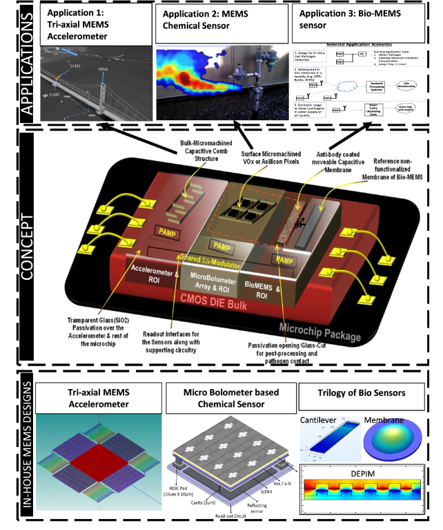
Monolithic CMOS MicroSystems for Structural , Chemical and Bio Hazard Detection (Completed)
FUNDING AGENCIES: |


|
|
| HIGH SPEED SIGNALING OVER ELECTRICAL INTERCONNECT |
|---|
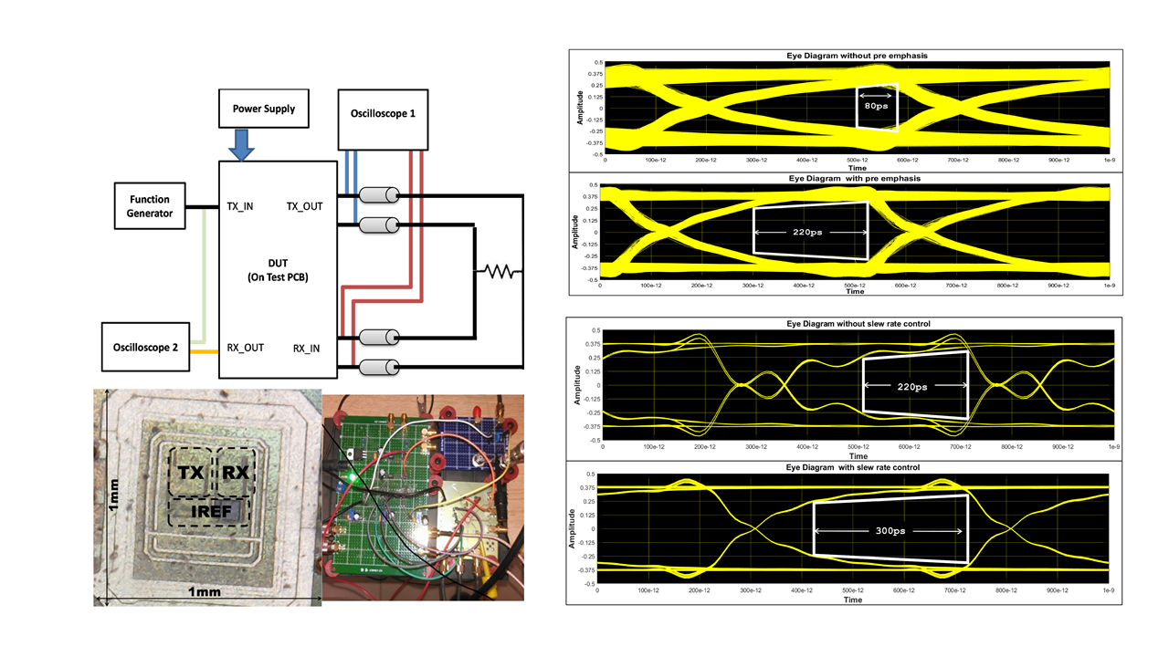
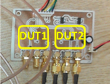
A Reconfigurable 2Gbps LVDS Transceiver 150nm/110nm CMOS
FUNDING AGENCY:
![]()
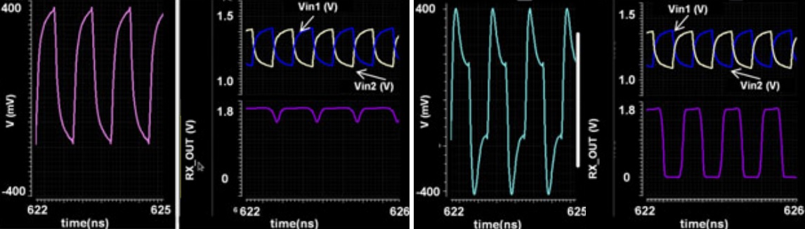
This project is based the design of Low-Voltage Differential-Signaling IOs (LVDS) in 150nm and 110nm CMOS processes for Flat-Panel Display operating at 2Gbps data-rate. LVDS signaling is now extensively used in Physical layers of numerous electronic components signaling over a longer physical medium to save power at higher data-rates. A 2Gbps LVDS transceiver in 150nm CMOS process was designed. The transceiver has embedded configurable pre-emphasis, slew-rate control and equalization. The pre-emphasis has been demonstrated to improve eye-opening at 2Gbps for longer channels of 10m while slew-rate control demonstrated improvement in eye-opening at 2Gbps for shorter channels in the presence of impedance discontinuities in the channel.The transceiver has integrated voltage and current biases, which reduce current variation of the transmitter to ±3% across the PVT corners (measured on 5 samples). Total power consumption of 16mW at 2Gbps with an improved FoM of 6.4pJ/bit was measured.
|
|
|
|
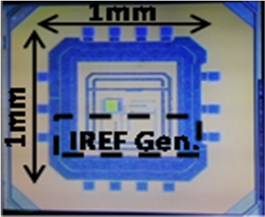
A PVT tolerant Current Reference Generator
FUNDING AGENCY:
![]()
A current reference circuit is an essential part of every autonomous IO limited integrated circuit. The mostly used approach to generate a stable current is to employ an external (off-chip) precision resistor with tolerance in ppm and produce a fixed voltage across this resistor through internal (on-chip) circuitry. Off-chip resistor is necessitated by the fact that on-chip resistors suffer from relatively large (20-30%) tolerances and therefore are not suitable for generating a stable reference current using this simple technique. In certain IO-limited applications, current variations in a simplistic on-chip current reference circuit due to PVT variations cause specification violation and in worst case outright functional failure. Therefore, it necessitates for a PVT tolerant compensated precision current reference to be designed for application specific integrated circuits.
|
|
|

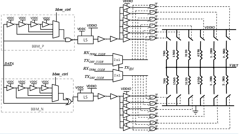
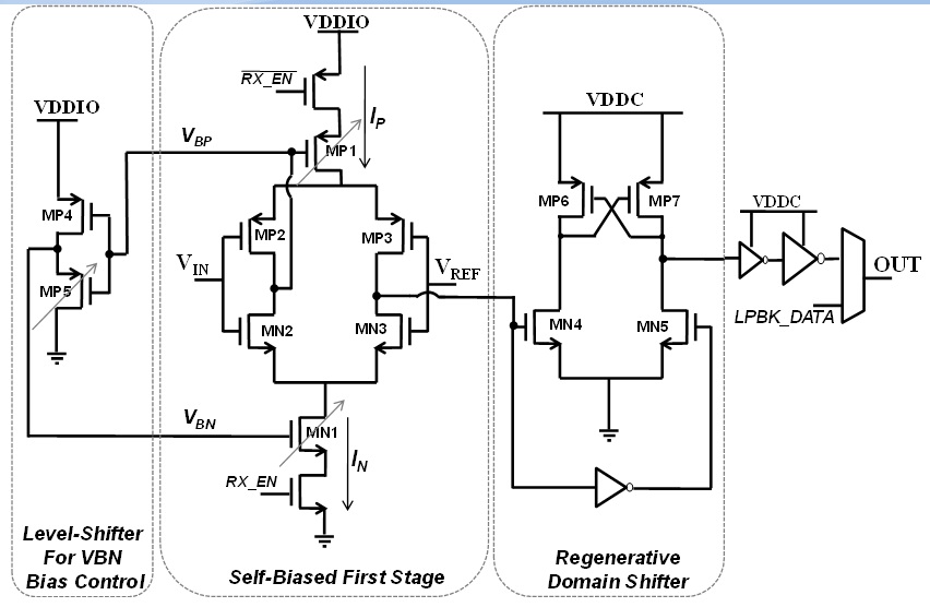
High-Speed IO design for DDR3/4 PHY
Currently DRAM interfaces incorporate a parallel single Ended signaling due to pin-out restrictions and backward compatibility [1-3]. So far the efforts to increase data rate of single ended signaling focus either on physical design and optimization, cross-talk cancellation techniques, noise reduction through encoding and supply insensitive design as well as decaps on bandwidth enhancement through equalization [4]. GDDR5, for instance, has achieved beyond 5Gbps using Data-Bus-Inversion (DBI), data training and data equalization. This, however, is leading the system to a fundamental limit to the performance set by cross talk, which eventually results in increased system cost due to additional components such as cross-talk equalizers [5] or other bandwidth improvement techniques [8-9] or because of increased inter-wire distances and shielding. Techniques such as parallel channels or fully buffered DIMMs are used to fulfill speed and capacity demands but again at the expense of system cost [1]. In due course, differential signaling with high speed serial IO enhancements is expected to potentially take over IO performances scaling post-DDR4. Another trend which is being exercised currently is to employ multi-mode transceivers in a PHY [7] to support multiple signaling standards using a single PHY. DDR4 and post-DDR4 future trends are moving towards a point to point configuration in which driver and receiver will have one-to-one interconnection.
This activity focuses on the design of combo DDR3 and DDR4 transceiver as part of a complete IO library containing power, ground and Vref IO cells.
|
|
|
|
|
| WIRELESS POWER TRANSFER |
|---|
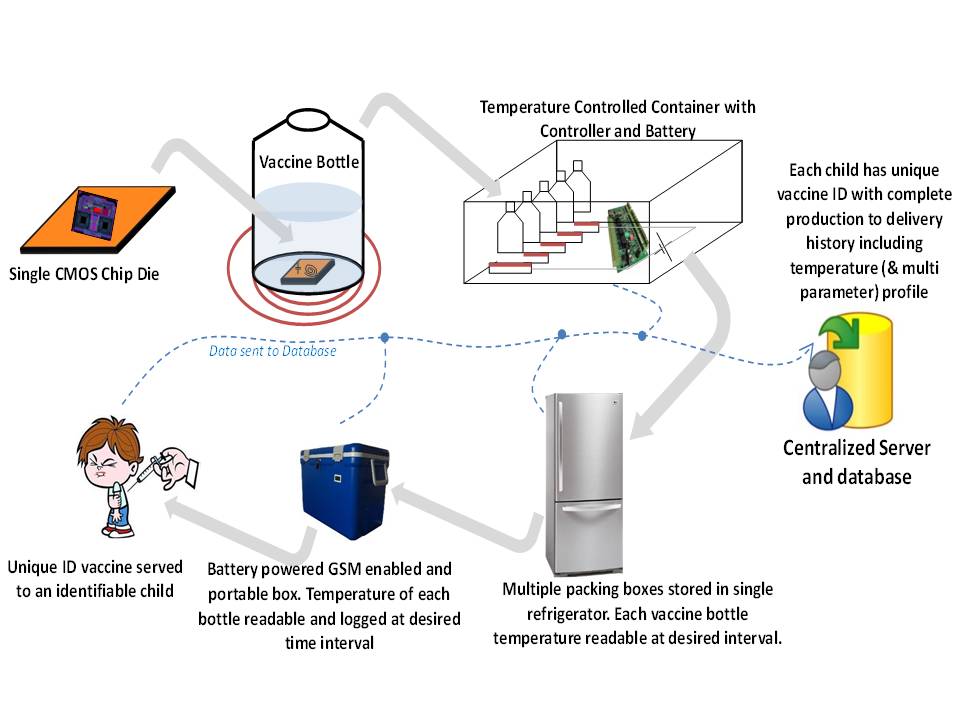
Vaccine Monitoring Microchip
FUNDING AGENCY:

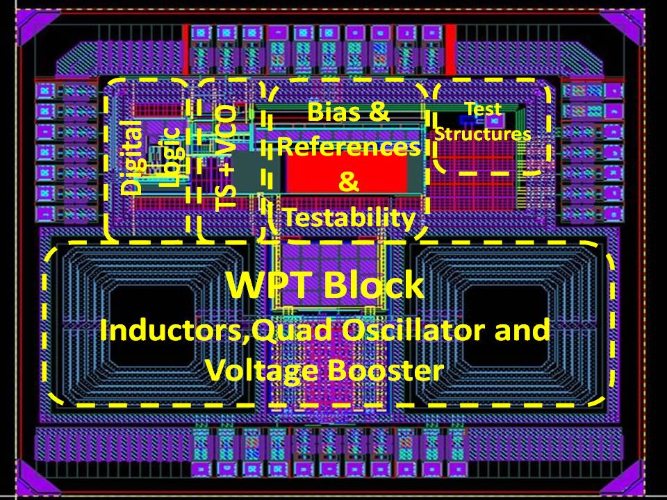
This project is based on a ground-breaking idea of using a CMOS wirelessly-powered microchip immersed directly in the vaccine to regularly monitor vaccine's fidelity from manufacturing to delivery. The global burden due to ineffective vaccines is in billions of USD and is one of the major issues in healthcare sector. This IC contains a novel wireless power transfer based on resonant power transfer concept with customized inductors especially designed for power-transfer at 200MHz. This IC also contains an ultra-low-power Temperature Sensor in Subthreshold operating region of the MOSFET with a power consumption of sub-nW. Several patents and publications are being applied through this project.
|
|
 |
 |
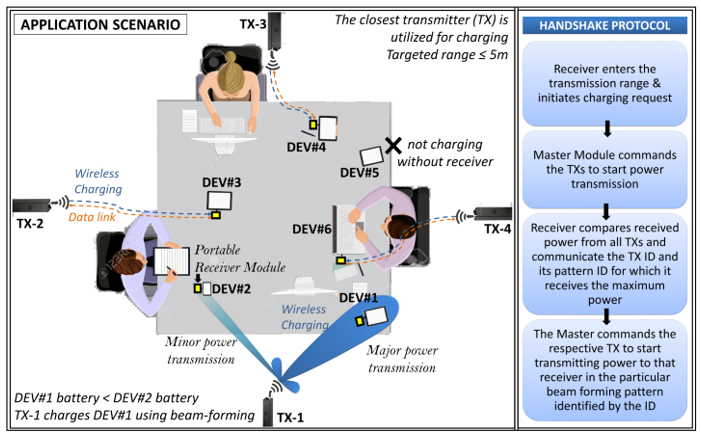
A Mid RANGE WIRELESS Power TRANSFER SYSTEM for portable electronic devices with BEAM forming (In-Progress)
FUNDING AGENCY:
![]()
A WPT system, which can be used for 1-5 Watts of Power over the air, at a distance of 5 meters with a power efficiency above 50%. The proposed system will use multiple wall-mounted transmitters (TX) and a portable small footprint receiver (RX). The main challenge in WPT is to reduce the size of TX and RX modules while achieving a reasonable efficiency over a reasonable distance. The focus of this work is to achieve a high power efficiency without transmitting a harmfully high power magnetic flux and with a portable footprint of the RX module. For this purpose, the proposed TX module would explore magnetic/dissipative transmission and employ beam-forming to enhance power directivity. The TX and RX would have embedded smartness to handshake and intelligently manage power transmission using beam-forming. The TX will have a relativelywall-mountable footprint (~50cmx50cm). The RX module would have a USB-pluggable footprint (10cmx5cm).
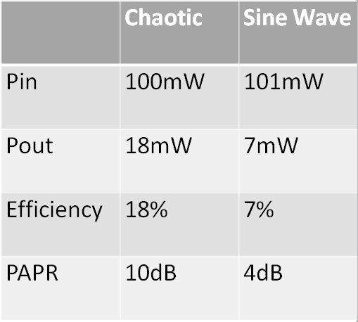
ENHANCED WIRELESS POWER TRANSFER
FUNDING AGENCY:
This work is focused on enhancing wireless power transfer techniques from different angles. One of the ideas being explored extensively is to avoid rectifier losses and devise a rectifier-less WPT circuit. Another angle shifts focus from the rectifier towards the wireless transmitter and attempts to apply chaotic signals to improve peak-to-average-power-ratio (PAPR) and therefore efficiently turn on/off the rectifying devices.
|
|
|
|
.jpg)
| ULTRA LOW POWER CIRCUITS |
|---|
ULTRA-LOW POWER DIGITAL CELLS
FUNDING AGENCY:
This work represents an IC designed for logic cells that exhibit significantly low-EDP and enhanced-NM than conventional cells. This was done exploiting Inverse Narrow Width Effect in Deep Submicron Process.These improvements were made possible by combining multiple design techniques of sizing and arranging the transistors. The design also exploited the exponential decreases in Vth in sub-threshold region. The improved cells were used to implement a medium-sized benchmark circuit, which was successfully fabricated and tested. The intrinsic capacitances of the NMOS(s) and PMOS(s) scale linearly with area. Exponential increase of subthreshold current competes against a linear increase in capacitances, an improved COC was achieved.
| HIGH SPEED, HIGH DENSITY DIGITAL BACKEND AND APR |
|---|
HIGH SPEED HIGH DENSITY APR OF ARBITRARY WAVE GENERATOR
FUNDING AGENCY:

A high speed digital back-end in the latest cutting edge technology of 45nm SOI CMOS. Arbitrary wave generator has 4Ghz clock, 64-bit DAC and Two 64-bit dual port memory array blocks of 4x4. SPI, LVDS, DAC, Interleave and Memory are the sub-block of the Digital block. Dedicated guided channel for high speed 4 GHz Clock.
Digital Block Top Level
AWG TOP LEVEL.
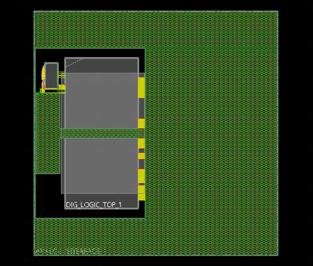
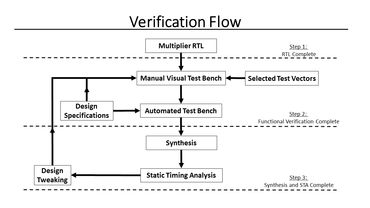
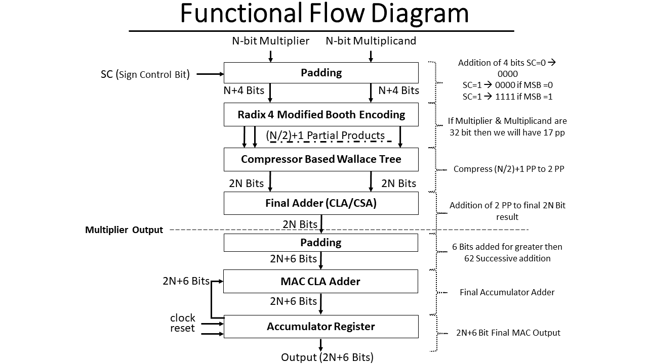
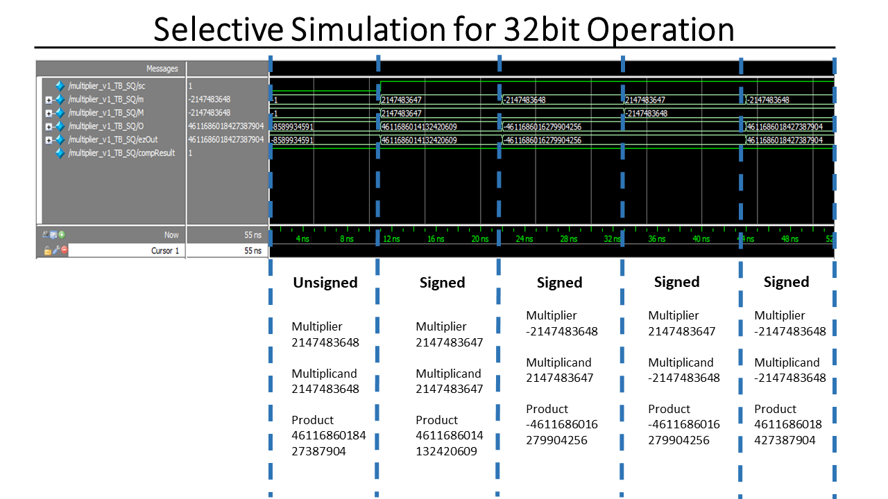
Multiply and Accumulate Unit
FUNDING AGENCY:


- Parameterized Signed/Unsigned Radix-4 MBE Multiplier and Accumulate Unit is designed.
-
Functional Verification performed on ModelSim software
-
Verification Methodology
- For 4 to 7-bit Operation: Manual TestBench and Automated TestBench results matched
- For 32-bit Operation: Results from Automated TestBench verified
-
Verification Methodology
-
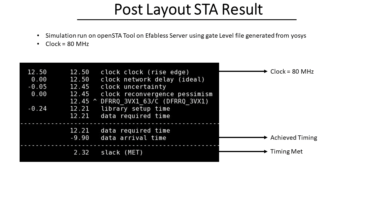
Layout and Post Layout Static Timing Analysis performed on Cadence Encounter and OpenSTA Tools:
- Using XFAB 180nm Technology.At 80MHz Clock Slack is Met.
| TEMPERATURE SENSOR |
|---|
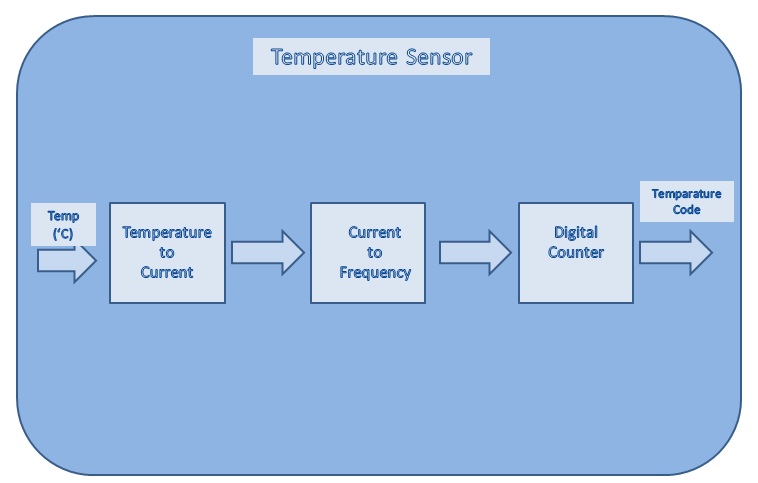
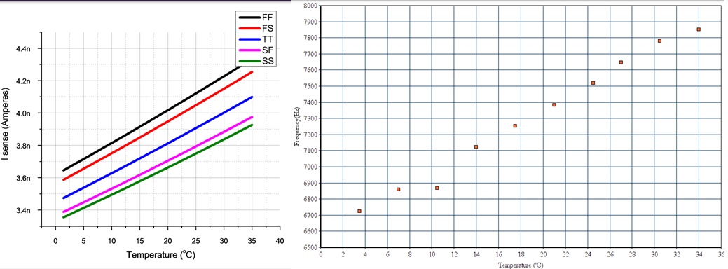
Ultra-Low Power Temperature Sensor
FUNDING AGENCY:
This project focusses on subthreshold circuit design for ultra-low-power temperature sensing. It is based on direct temperature to frequency conversion using ultra-low-power VCOs. A supply and process invariant temperature sensing in subthreshold region is one of the main design challenges. Combining temperature sensing and VCO in a single loop is also the mai focus of this work.
|
|
|
| LAB-ON-A-CHIP |
|---|
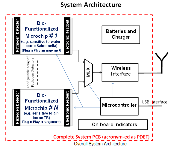
Realtime Pathogen detector System
This project is based on the idea of removing the time-hurdle in the real-time detection of a pathogen in out-of-the-lab settings without expensive instruments to open up the possibility of mass-scale domestication. The core of this project is based on a BioMEMS IC with a pathogen-sensitive capacitive-front-end and a low-power, low-noise signal-pickup chain followed by a wireless communication stack. This project is focused on detecting both air-borne and water-borne pathogens in public places or inside houses and communicating the detection of pathogen to the neighboring smart devices to trigger a preventive response.
|
|
| Fifth Generation Cellular Network - (5G) |
|---|
RF Transceiver Design for 5G
This project aims at answering an important open question related to the effective spectrum usage in the physical layer of the 5th Generation (5G) mobile systems by incorporating an In-band Full-Duplex (IBFD) transceiver architecture. FD radio technology, where the devices transmit and receive signals simultaneously at the same center frequency, is the new breakthrough in wireless communications. This unconventional scheme for radio links promises to theoretically double the spectral efficiency compared to conventional Half-Duplex (HD) systems. A possible implication of such a revolutionary approach in wireless communications is that the cellular networks can effectively reduce their spectrum requirements by half. Moreover, advantages in higher network layers as well such as: low latency, collision prevention and security has drawn significant attention in the design of IBFD systems.
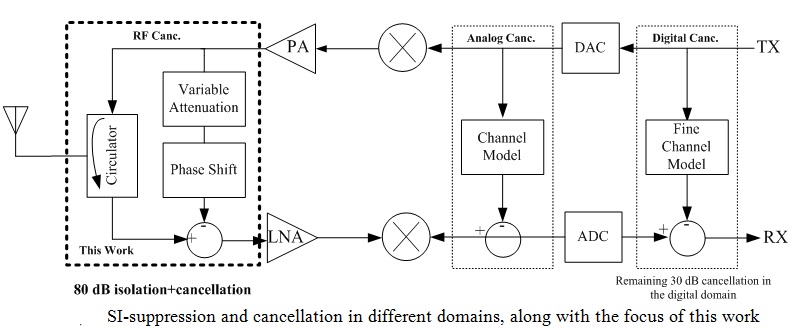
The biggest obstacle in the path of practical realization and implementation of small and low cost IBFD transceivers is the strong in-band interference, also termed as self-interference (SI). The self-interference is a result of either incorporating a single antenna for both transmission/reception or employing separate but closely spaced antennas, as a result of which the transmit signal couples strongly to the receive path. Fig.1 illustrates the different paths from which the transmit signal can couple to the receiver and saturate it. This coupling can be 60−100 dB stronger than the desired received signal, depending on the transmitted power and antenna isolation. In principle the SI can be completely cancelled at the receiving end, prior to low noise amplification, by subtracting the already known transmitted data within the device from the received signal.
|
|
|
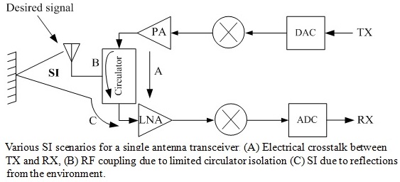
The SI cancellation, however, is not as straightforward as it appears to be, since the original transmitted signal radiating from the antenna experiences various amounts of attenuation and delays, depending on the channel characteristics between the transmitter and the receiver, before falling into the receiver as linear SI components. Moreover, the non-linearities associated with the transmitting chain particularly that of the Power Amplifier (PA) generates harmonic contents which also fall in the receiver along with the linear SI components. The non-linearities associated with the receiver is also a matter of concern, as the transceiver non-linearities can mix with each other and generate intermodulation and cross modulation distortion products. To make matters worse the transmitter noise generated by high power components in the transmitting chain referred to as broadband noise increases the receiver’s noise floor to levels as high as 40−50 dB.
| Developed Systems and Prototypes |
|---|
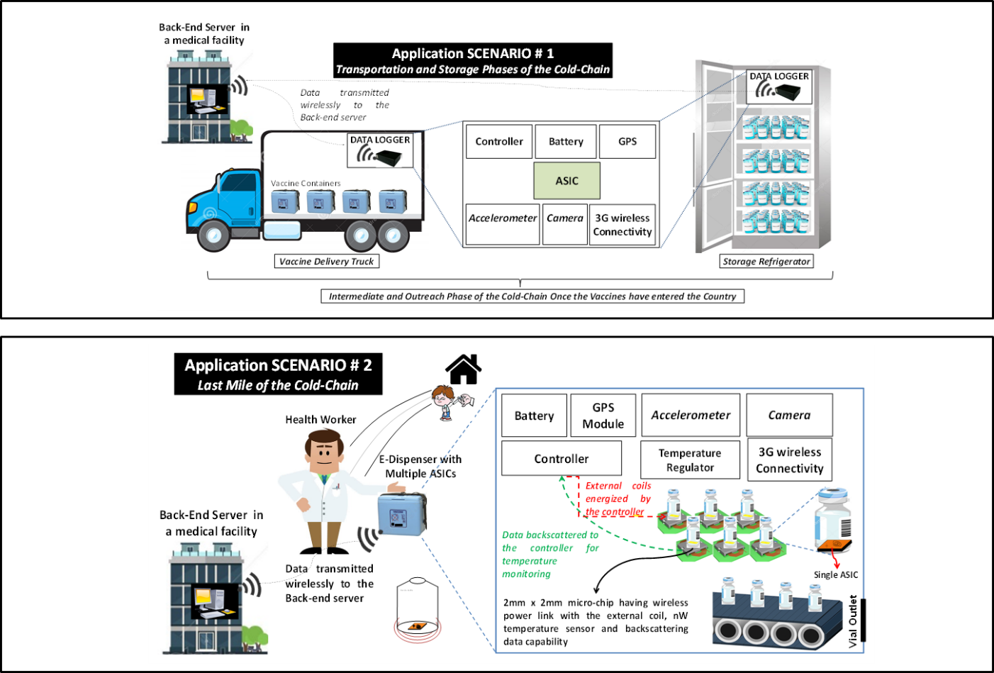
Portable, Low-Cost and Smart Electronic Data-Logger and Dispenser for Vaccine Cold-Chain
A smart electronic system which can be used in two modes; 1) as a low-cost data-logger for different phases of the vaccine cold-chain and 2) as a multi-feature electronically controlled vaccine dispenser to enhance the last-mile transportation and delivery. This system is based on a novel method to measure and record the temperature as part of a multi-parameter log and then use that log to rectify the issues with the vaccine transportation-and-storage-chain and also to improve the yield of the delivered vaccines with an automated EMR generation at a backend system. An application-specific IC (ASIC), which would either be immersed in or pasted at the bottom of each vaccine vial or integrated within a portable low-cost data-logger, would be at the core of the ultra-low-power temperature sensing. This ASIC would be powered-up through a wireless-power-transfer circuit just like an RFID-tag, therefore, it can be considered as a custom-designed RFID tag for this application.
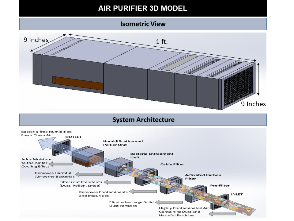
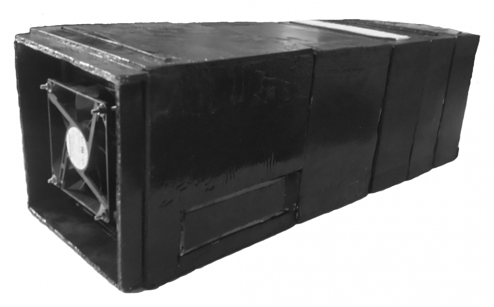
Smart-Portable-Scalable Electronic Air Purifier
A portable, low-cost and scalable Electronic Air-Purifier (AP) suitable for effective environment control of a typical-sized (~25m2) confined room in an office or at home. Custom built with plug-n-play functional-compartments including; implementing dust-filtering, odor removal, fine particulate removal, electrostatic bacterial entrapment, UV bacterial inactivation, temperature and humidity control along with a continuous status update of the Air-Quality in the confined space through its application.
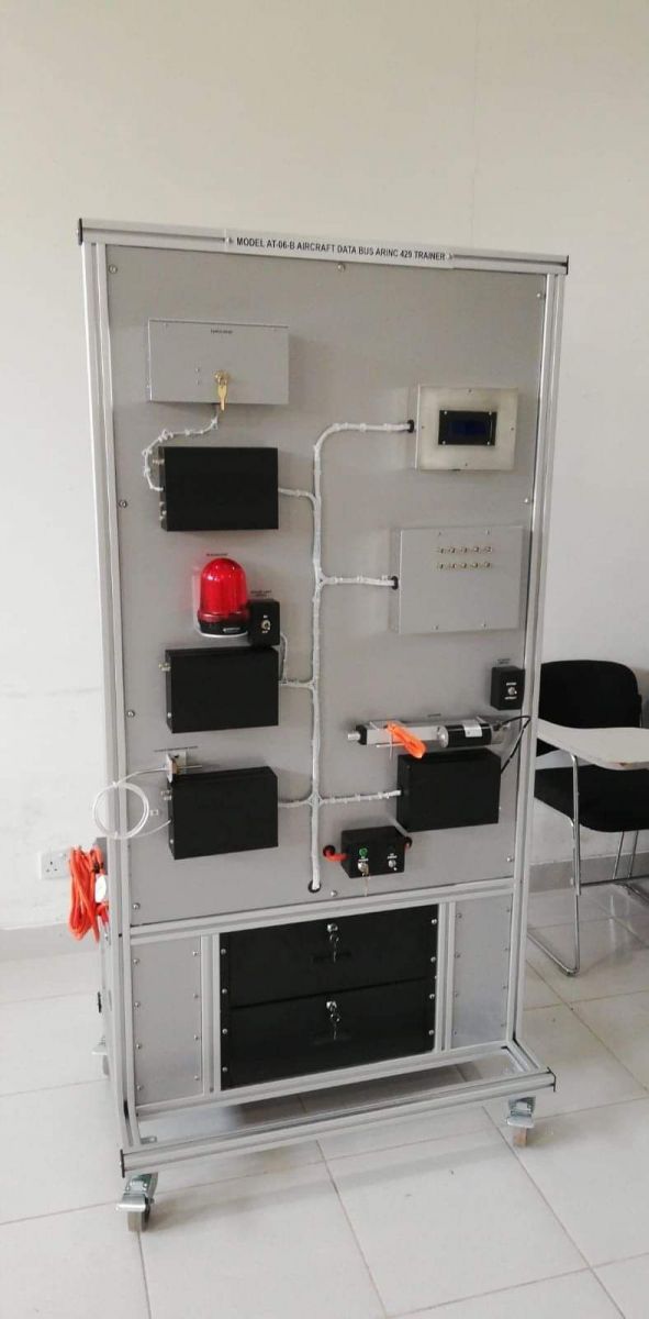
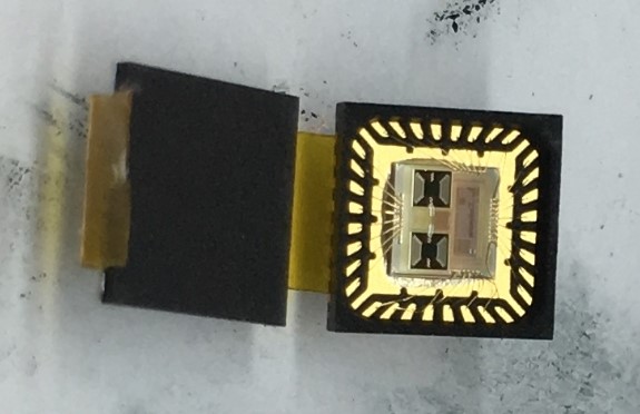
Arinc 429 Trainer
FUNDING AGENCY:
![]()
An ARINC-429 Avionics Interface Bus Trainer was designed, manufactured, integrated and successfully tested in collaboration with Aero Train - USA. ARINC-429 is a high-fidelity Avionics-Bus custom-designed for intra-aircraft wired-communication, therefore, it employs a peculiar communication protocol and physical level high-voltage impedance-matched signaling. Designed to train students and personnel to data transmission and bus standards used in commercial and transport aircraft. Features include, Linear Actuator, Rotating Beacon, Outside Air Temperature Probe and Cargo Door.